Jigsaw Machine
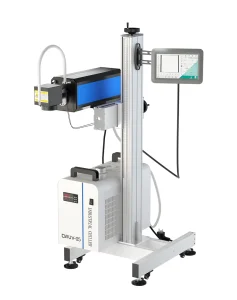
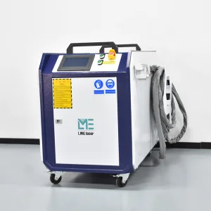
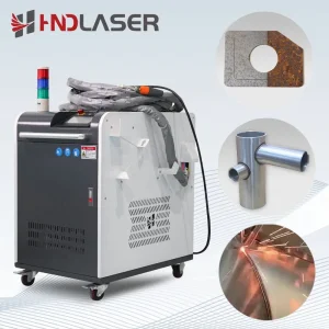
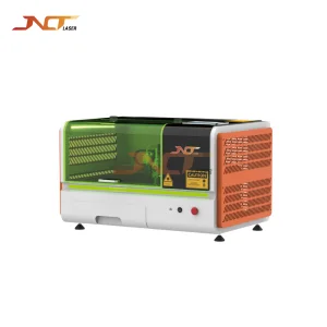
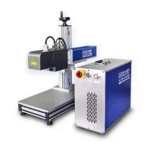
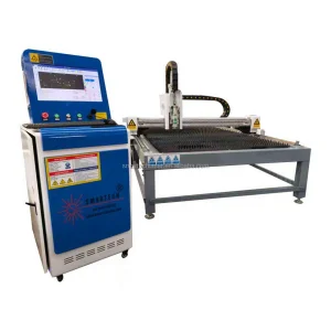
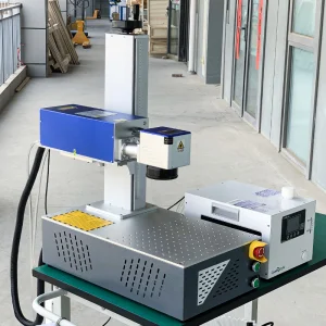
As electronic components shrink into sub-millimeter scales, high-energy 355nm ultraviolet (UV) lasers are replacing conventional photothermal infrared fiber and CO2 laser architectures to eliminate Heat-Affected Zones (HAZ) and edge thermal degradation.
Driven by System-in-Package (SiP) and Advanced High-Density Interconnect (HDI) PCBs, OEM UV laser cutting systems deliver burr-free singulation of flexible printed circuits (FPC), ultra-thin wafer dicing, and ceramic substrate micro-vias without mechanical stress.
Precision cutting of bio-compatible polymers (polyimide, PTFE, bio-resorbable stents) requires zero carbonization. UV photolytic bond breaking prevents toxic off-gassing and edge melting, satisfying FDA bio-device manufacturing protocols.
As tier-1 system integrators shift toward automated modular factories, enterprise buyers demand standardized OEM/ODM laser equipment platforms with integrated machine vision (CCD AOI), real-time power stabilization, and Industry 4.0 IoT telemetry.
Understanding why 355nm UV laser wavelengths outperform thermal 1064nm Fiber and 10.6µm CO2 lasers in high-precision micro-manufacturing environments.
Traditional infrared lasers cut materials by thermal melting (photothermal reaction), leaving micro-cracks, carbonized edges, and structural thermal distortion. Ultraviolet lasers emit high-energy photons (3.49 eV at 355nm) that directly break the chemical bonds of molecular compounds (photolytic reaction). This "cold processing" mechanism causes target molecules to vaporize instantaneously into micro-gas particles without transferring thermal kinetic energy to adjacent matrix walls.
Due to diffraction-limited optics, the theoretical minimum focal spot size ($d$) is directly proportional to wavelength ($\lambda$). Because $\lambda_{UV} = 355\text{ nm}$ is one-third that of fiber lasers ($1064\text{ nm}$), UV optical systems achieve focal beam spots under 5 to 10 micrometers. This enables sub-micron precision contour cutting, micro-vias drilling down to $15\mu\text{m}$ diameter, and zero-clearance component separation.
Modern OEM UV laser machinery integrates nanosecond (ns), picosecond (ps), and femtosecond (fs) Diode-Pumped Solid-State (DPSS) laser sources. Ultra-short pulse durations restrict energy dissipation within a timeframe faster than the electron-phonon relaxation time, virtually eliminating the Heat-Affected Zone (HAZ < 2µm) even on sensitive multi-layer materials like coverlay polyimide and copper foils.
| Laser Wavelength & Type | Primary Processing Mechanism | Heat Affected Zone (HAZ) | Min Kerf Width | Target Substrates | Edge Carbonization |
|---|---|---|---|---|---|
| 355nm UV DPSS (Nanosecond) | Photolytic / Photo-chemical | < 5 µm | 10–15 µm | FPC, PI, Coverlay, PET, Ceramics | Negligible |
| 355nm UV Picosecond / Femtosecond | Cold Ablation / Multiphoton | < 1 µm (Zero HAZ) | 3–8 µm | Glass, Sapphire, Wafer Dicing, OLED Screen | Zero Carbonization |
| 1064nm Fiber Laser | Photothermal Melting | 30–100 µm | 40–80 µm | Thick Metals, Carbon Steel, Stainless Steel | High Thermal Impact |
| 10.6µm CO2 Laser | Thermal Evaporation | > 100 µm | 100–250 µm | Acrylic, Wood, Heavy Organic Plastics | Severe Edge Melting |
Tailored engineering implementations across major regional manufacturing hubs.
High-volume manufacturing lines in East Asia utilize fully automated UV laser depaneling cells equipped with dynamic linear motor stages (up to 2000 mm/s) and CCD vision software. These systems cut Rigid-Flex PCBs, camera module substrates, and 5G antenna assemblies with zero physical strain on delicate micro-components.
European tier-1 automotive suppliers deploy UV laser cutters for micro-machining automotive radar substrates, battery management system (BMS) busbars, and glass-filled resin housings. In healthcare technology, UV laser micro-hole drilling creates microfluidic channels in diagnostic lab-on-a-chip devices.
North American aerospace operations utilize high-power nanosecond and picosecond UV lasers for precision stripping of specialized insulation coatings, micro-drilling carbon-fiber reinforced polyimides, and pattern scribing thin-film solar cells for orbital satellites.
Pioneering precision machinery R&D, automated manufacturing lines, and international quality management standards.
Founded in May 2010, Chengdu Jigsaw Machine Co., Ltd. is a high-tech enterprise specializing in the research and development, manufacturing, sales, and service of industrial sawing, cutting, and laser precision processing equipment. With years of experience in the field of cutting machinery and industrial automation, the company is committed to providing efficient, reliable, and intelligent cutting solutions for global customers across a wide range of industries.
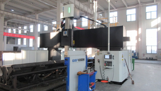
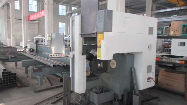
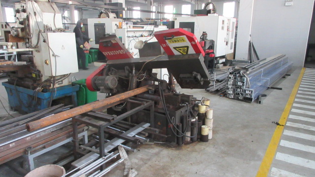
The company’s main product portfolio includes precision UV laser cutting systems, fiber laser welding and cleaning platforms, handheld jigsaw machines, industrial reciprocating saws, CNC sawing and cutting systems, automated cutting production lines, gantry-type heavy-duty cutting machines, tube and profile cutting equipment, as well as intelligent feeding systems and customized automation solutions. These products are widely used in electronics manufacturing, semiconductor packaging, woodworking, metal fabrication, construction, furniture manufacturing, and general industrial processing.
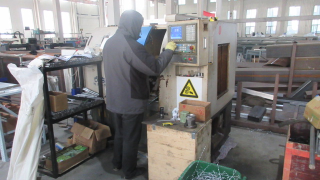
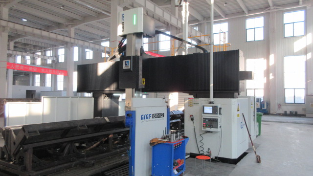
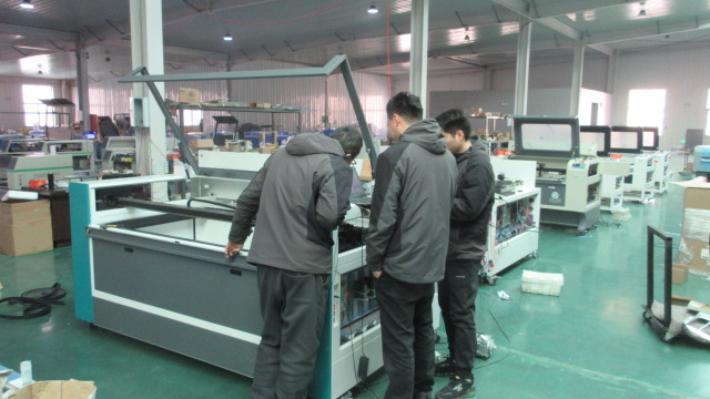
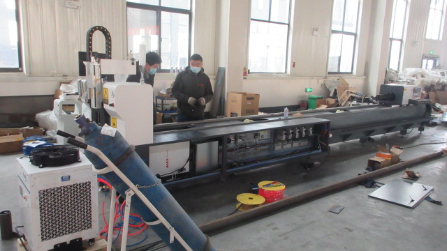
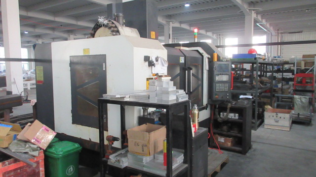
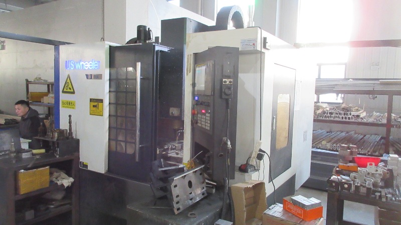
Chengdu Jigsaw Machine Co., Ltd. operates a modern production facility covering over 2,000 square meters, equipped with advanced machining, assembly, and testing systems. The company has established a strong domestic and international distribution network, with partners and agents in multiple countries and regions, enabling timely technical support and comprehensive after-sales service for customers worldwide.
Since its establishment, the company has continuously focused on innovation and resource integration in R&D, manufacturing, and application development. It has obtained ISO9001 international quality management system certification and CE certification, ensuring that all products meet strict international standards for quality, safety, and performance. Guided by the spirit of "precision manufacturing and pursuit of excellence," Chengdu Jigsaw Machine Co., Ltd. adheres to a development philosophy of continuous innovation and practical advancement.
Where precision UV micro-processing is heading over the next decade.
Transitioning from nanosecond pulse profiles to femtosecond pulses ($< 500\text{ fs}$) allows zero-heat dissipation cutting of glass, quartz, and multi-layer sapphire without structural micro-cracking.
Integrating real-time machine learning vision algorithms directly onto galvo scanning heads to dynamically compensate for material warp, thermal expansion, and non-linear contour distortions.
Automatic power attenuation feedback loops guarantee photon fluence density stability within $\pm 0.5\%$, optimizing production yield rates for high-reliability medical and defense components.
Continuous roll-to-roll laser cutting modules tailored for flexible electronics, solar cell thin-films, and wearable diagnostic sensors, supporting ultra-high throughput assembly lines.
In-depth answers from our senior optical engineering and OEM system design team.
Flexible Printed Circuit (FPC) boards consist of delicate layers of polyimide (PI), adhesive, and thin copper foil. A 1064nm fiber laser cuts by generating intense thermal heat, which causes edge melting, copper delamination, and carbonized black edges (large Heat-Affected Zone). The 355nm UV laser cuts via photolytic cold processing, breaking molecular bonds directly. This results in razor-sharp, burr-free edges with zero thermal damage to adjacent micro-circuits.
We provide comprehensive turnkey OEM/ODM engineering services, including custom laser optical path design, choice of nanosecond/picosecond DPSS laser engines (3W to 25W+), dynamic 3D galvo optical scanners, custom linear motor motion stages (granite bed stability), tailored machine vision (CCD AOI alignment software), automatic load/unload robotic handling, and custom enclosure dimensions matching ISO cleanroom standards.
Modern solid-state UV laser sources feature diode module operational lifespans exceeding 20,000 to 30,000 hours. To maintain optimal beam quality ($M^2 < 1.2$), optical harmonic generator crystals (THG crystals) and F-theta lenses require periodic inspect-and-clean protocols every 3,000 hours. Our automated machines include sealed optical paths with positive pressure dust-free filtration to maximize optical element longevity.
Our high-resolution CCD cameras capture pre-etched Fiducial alignment marks on substrates prior to laser firing. The integrated AI vision software calculates translational ($X, Y$) and rotational ($\theta$) offsets down to sub-micron accuracy, automatically updating the galvo scan vectors in real-time. This eliminates fixture placement errors and guarantees cut position repeatability of $\pm 2\mu\text{m}$.
All UV laser machines manufactured by Chengdu Jigsaw Machine Co., Ltd. strictly comply with CE safety directives, ISO9001 quality standards, and International Electrotechnical Commission (IEC 60825-1) Laser Safety Standards. Systems feature fully enclosed Class 1 laser safety housings, safety interlocks, optical viewing windows, and integrated high-efficiency fume extraction ports.